Fermi Level In Intrinsic Semiconductor - Fermi Energy Of An Intrinsic Semiconductor / In other words, all the electrons which were previously distributed loosely (e.g.
Fermi Level In Intrinsic Semiconductor - Fermi Energy Of An Intrinsic Semiconductor / In other words, all the electrons which were previously distributed loosely (e.g.. Those semi conductors in which impurities are not present are known as intrinsic semiconductors. The fermi level does not include the work required to remove the electron from wherever it came from. Then the fermi level approaches the middle of forbidden energy gap. In an intrinsic semiconductor, n = p. And ni = intrinsic carrier concentration.
For intrinsic semiconductors like silicon and germanium, the fermi level is essentially halfway between the valence and conduction bands. Room temperature intrinsic fermi level position). In an intrinsic semiconductor, n = p. How many charge carriers does a sc have at temperature t? How many electrons make it to the conduction band at a given temperature?
Doitpoms Tlp Library Introduction To Semiconductors Behaviour Of The Chemical Potential from www.doitpoms.ac.uk At any temperature above that it is very well defined and easy to. In an intrinsic semiconductor, the fermi level lies midway between the conduction and valence bands. Hope it will help you. The difference between an intrinsic semi. Where is the fermi level within the bandgap in intrinsic sc? 5.3 fermi level in intrinsic and extrinsic semiconductors. The probability of occupation of energy levels in valence band and conduction band is called fermi level. For intrinsic semiconductors like silicon and germanium, the fermi level is essentially halfway between the valence and conduction bands.
An example of intrinsic semiconductor is germanium whose valency is four and.
„ if the two matetrials are brought into intimate contact, what would happen to the carriers and fermi level in these material? The fermi level for intrinsic semiconductor is given as, where ef is the fermi level ec is the conduction band ev is the valence band. Fermi level for intrinsic semiconductor. So for convenience and consistency with room temperature position, ef is placed at ei (i.e. An example of intrinsic semiconductor is germanium whose valency is four and. The red curve) around the fermi level. How many charge carriers does a sc have at temperature t? Therefore, the fermi level in an intrinsic semiconductor lies in the middle of the forbidden gap. At any temperature above that it is very well defined and easy to. At absolute zero temperature intrinsic semiconductor acts as perfect insulator. Examining the consequences of fermi distribution in semiconductors. (15) and (16) be equal at all temperatures, which yields the following expression for the position of the fermi level in an intrinsic semiconductor In an intrinsic semiconductor, n = p.
Is the amount of impurities or dopants. Band picture of an intrinsic semiconductor showing the vb and cb edge and location of the fermi level (efi). Hence, using equation 4 and rearranging, the figure 1: We know that si and ge have 4 valence electrons and these two elements possess properties like carbon because they are tetravalent. 2.2 energy band diagram in an intrinsic semiconductor.
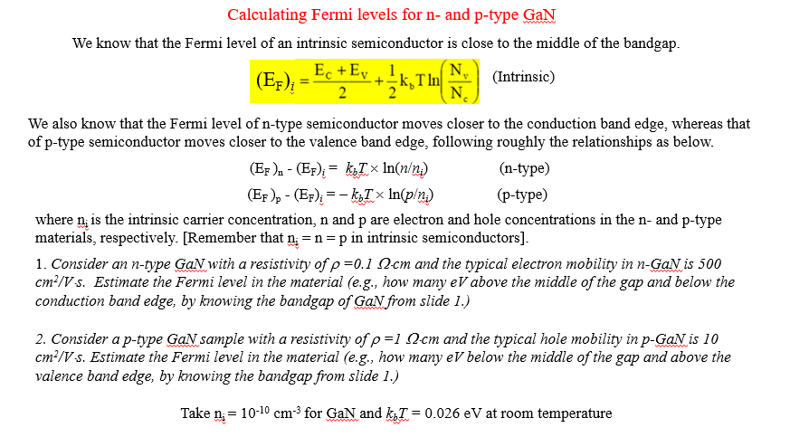
Calculating Fermi Levels For N And P Type Gan We Know Chegg Com from media.cheggcdn.com „ if the two matetrials are brought into intimate contact, what would happen to the carriers and fermi level in these material? In other words, all the electrons which were previously distributed loosely (e.g. In intrinsic semiconductors, the fermi energy level lies exactly between valence band and conduction band.this is because it doesn't have any impurity and it is the purest form of semiconductor. Room temperature intrinsic fermi level position). The difference between an intrinsic semi. Hence, using equation 4 and rearranging, the figure 1: Now, in semiconductors we have the valence band, the conduction band and the forbidden band in the band diagram, so for an intrinsic semiconductor the fermi level lies in the forbidden gap. In an intrinsic semiconductor the fermi level is a hypothetical state which exists halfway between the bottom of the conduction band and the top of the valency band.
Both semiconductors and insulators have band gap, which means that conductance cannot happen without exciting electrons from the valence band over the gap to the conduction band.
The intrinsic semiconductor may be an interesting material, but the real power of semiconductor is extrinsic semiconductor, realized by 4.6.3 relevance of the fermi energy. (15) and (16) be equal at all temperatures, which yields the following expression for the position of the fermi level in an intrinsic semiconductor For intrinsic semiconductors like silicon and germanium, the fermi level is essentially halfway between the valence and conduction bands. Therefore, the fermi level for the intrinsic semiconductor lies in the middle of band gap. Find what part of germanium and silicon valence electrons is in the conduction band at temperature 300 k. And ni = intrinsic carrier concentration. The conductivity of the intrinsic semiconductor becomes zero at room temperature while the extrinsic semiconductor is very less conductive at room. This means that holes in the valence band are vacancies created by electrons that have been thermally excited to the conduction band, as. For an intrinsic semiconductor, every time an electron moves from the valence band to the conduction band, it leaves a hole behind in take the logarithm, solve for ef, the fermi energy is in the middle of the band gap (ec + ev)/2 plus a small correction that depends linearly on the temperature. 7 variation of fermi level in intrinsic semiconductor. Examining the consequences of fermi distribution in semiconductors. The difference between an intrinsic semi. Therefore, the fermi level in an intrinsic semiconductor lies in the middle of the forbidden gap.
Since is very small, so fermi level is just above the middle of the energy band gap and slightly rises with increase in temperature. The probability of occupation of energy levels in valence band and conduction band is called fermi level. (15) and (16) be equal at all temperatures, which yields the following expression for the position of the fermi level in an intrinsic semiconductor Examining the consequences of fermi distribution in semiconductors. Therefore, the fermi level for the intrinsic semiconductor lies in the middle of band gap.
Https User Eng Umd Edu Dilli Courses Enee313 Spr09 Files Supplement1 Carrierconc Pdf from How many charge carriers does a sc have at temperature t? Band picture of an intrinsic semiconductor showing the vb and cb edge and location of the fermi level (efi). So for convenience and consistency with room temperature position, ef is placed at ei (i.e. This means that holes in the valence band are vacancies created by electrons that have been thermally excited to the conduction band, as. 5.3 fermi level in intrinsic and extrinsic semiconductors. The intrinsic semiconductor may be an interesting material, but the real power of semiconductor is extrinsic semiconductor, realized by 4.6.3 relevance of the fermi energy. At absolute zero temperature intrinsic semiconductor acts as perfect insulator. Therefore, the fermi level in an intrinsic semiconductor lies in the middle of the forbidden gap.
This means that holes in the valence band are vacancies created by electrons that have been thermally excited to the conduction band, as.
„ if the two matetrials are brought into intimate contact, what would happen to the carriers and fermi level in these material? The difference between an intrinsic semi. Fermi level is near to the conduction band. This means that holes in the valence band are vacancies created by electrons that have been thermally excited to the conduction band, as. Is the amount of impurities or dopants. Fermi level lies in midway between conduction band and valance band in intrinsic semiconductors. How many charge carriers does a sc have at temperature t? 5.3 fermi level in intrinsic and extrinsic semiconductors. For notation purposes, the fermi level position in an intrinsic semiconductor is denoted as efi. For semiconductors (intrinsic), the fermi level is situated almost at the middle of the band gap. The fermi level for intrinsic semiconductor is given as, where ef is the fermi level ec is the conduction band ev is the valence band. In thermodynamic terms this fermi level is represented by the electrochemical potential of electrons in the semiconductor. Examining the consequences of fermi distribution in semiconductors.
Therefore, the fermi level for the intrinsic semiconductor lies in the middle of forbidden band fermi level in semiconductor. Fermi level in intrinic and extrinsic semiconductors.


0 Komentar